|
Tricorder Project
2021
Support documentation and discussions for the Tricorder project.
|


|
|
Tricorder Project
2021
Support documentation and discussions for the Tricorder project.
|
|
The Tricorder is a multipurpose environmental sensing device, as shown on Star Trek. The TV show prop, which is shown in the image below, is a handheld hinged device with a display and a variety of buttons and lights.

Despite significant advances in wearable technology in the past several years, there is a lacking of readily accessible technology that can provide feedback about a someone's immediate environment. The biggest problem with environmental sensors in personal and wearable electronics is that close proximity to the human body will almost certainly interfere with most sensor readings. For example, if an Apple Watch were to contain a temperature sensor in order to sense the ambient air temperature, such a measurement would be rendered inaccurate by the device's close proximity to the human body. Therefore, it is mostly impractical to integrate environmental sensors into existing personal electronics, like smartphones and smartwatches. My goal in this project is to not only emulate the prop used in the TV show, but to also create a functioning device that can provide feedback to me about the environment.
The sensors and components I wish to include in this device are:
When I began this project in 2018, I had little experience in programming and electronics. In addition, I wanted to develop my skills in designing parts specifically for 3D printing. I decided that for a first prototype, a hinged device in a small, handheld form factor would be too ambitious for my skillset. Therefore, I started by designing a device after a different, larger Star Trek prop. The prototype, shown below in comparison to its TV show prop counterpart, was 3D printed and (crudely) painted to mimic the contours on the TV prop.
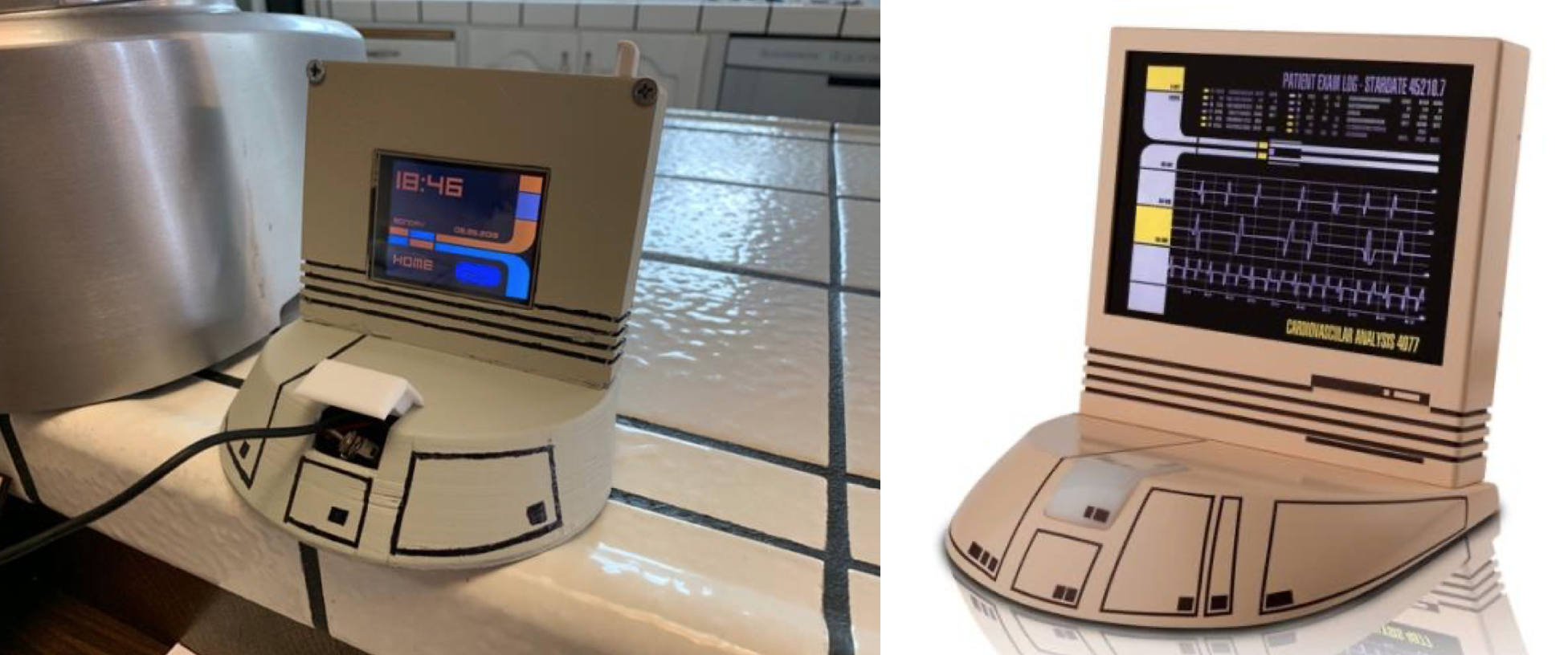
The device was primarily an alarm clock that kept time using a DS3231 Real Time Clock module. It also measured temperature, pressure, and humidity using a BME280 sensor module. Inside the device, an Arduino Uno communicated with these sensors using I2C. The display interface is a 3.2-inch LCD that was driven using the Adafruit Graphics Library. Finally, I powered the device with a salvaged cell phone battery with a lithium polymer battery charging module. Shown in the photo below, the white cap on the device can be removed to charge the battery and toggle the on/off switch.
The biggest problem with this prototype was its crudeness. Without experience in soldering, the inside of the device was a mess of jumper wires and loose connections. In addition, the 3D printed pieces of the enclosure did not fit well together. Finally, the device was very slow. The Adafruit Graphics Library provides some excellent building blocks for displaying shapes and text, but it contains blocking code that made the GUI painfully slow, especially with the Arduino Uno's 8 MHz ATmega328 microcontroller.
This device used the exact same components as the first one, except I switched to an Arduino Nano. In addition, I added a small piezo buzzer to improve the user interface. I also decided to temporarily proceed without battery power. I found myself using the device mostly as a stationary clock on my desk, so I didn't feel the need to make it mobile with battery power yet.
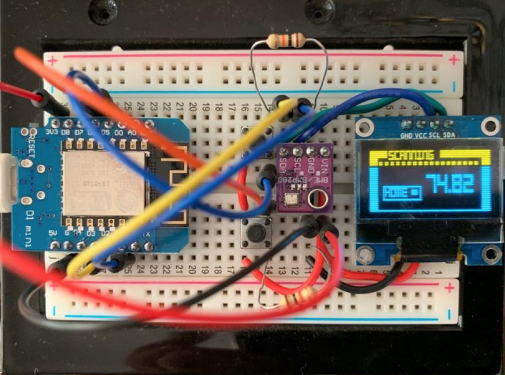
This prototype was inspired by a slightly different TV show prop that I found much easier to replicate in CAD. With improved design skills, I was able to more closely model the different features of the TV prop. More importantly, this design was much sturdier. As I became more confident in my soldering abilities, I was able to solder the Arduino Nano development board, along with the RTC, and temperature modules, to a single prototyping board. Eliminating all the jumper wires made the device much more durable. The image below shows the internal electronics inside the second prototype.
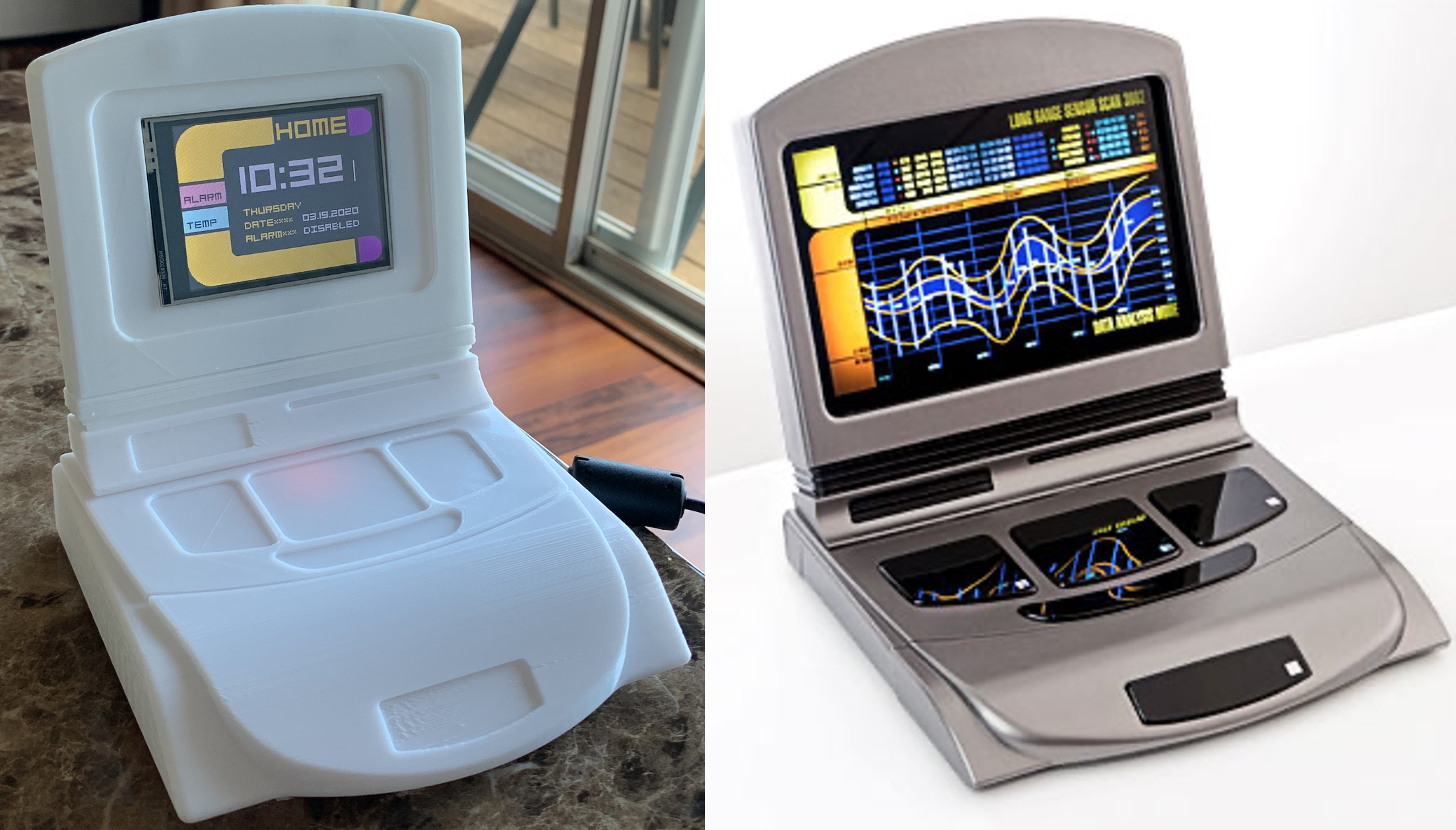
I was able to improve the speed of the device by structuring the screen navigation as a finite state machine and implementing a simple task scheduler.
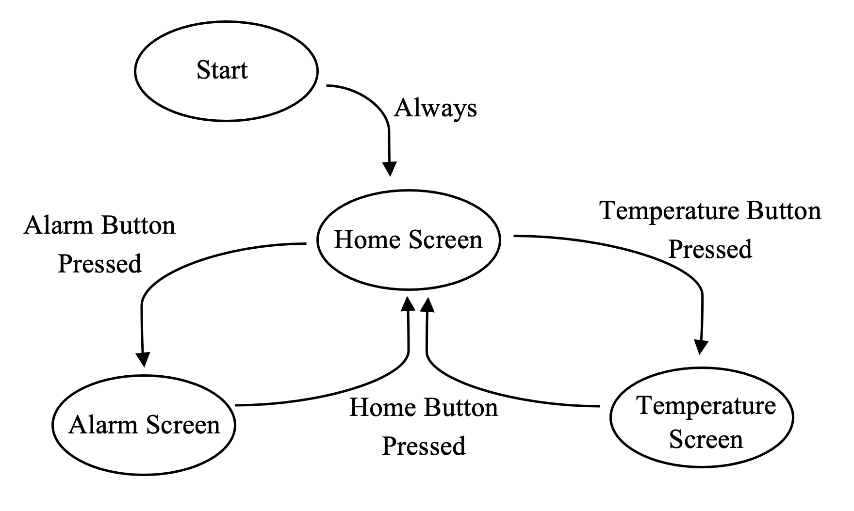
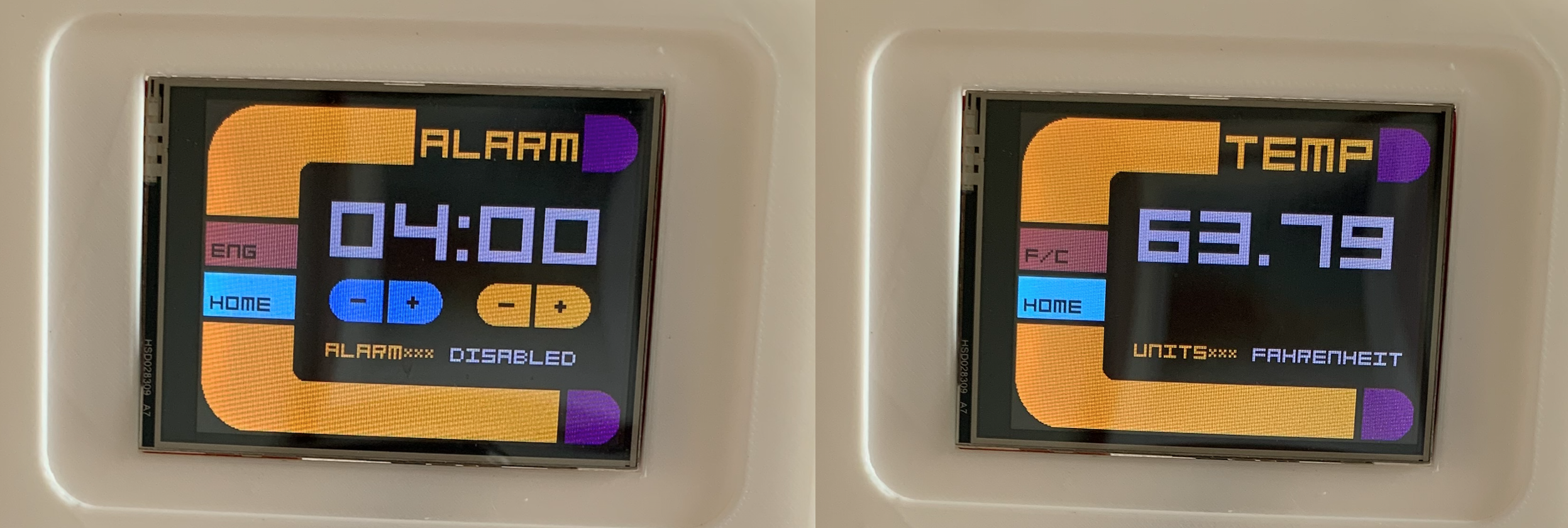
Using the state transition diagram above, there are a series of tasks that run at different intervals depending on which screen is active. The image below shows the other screens of the GUI.
The different tasks in the GUI are:
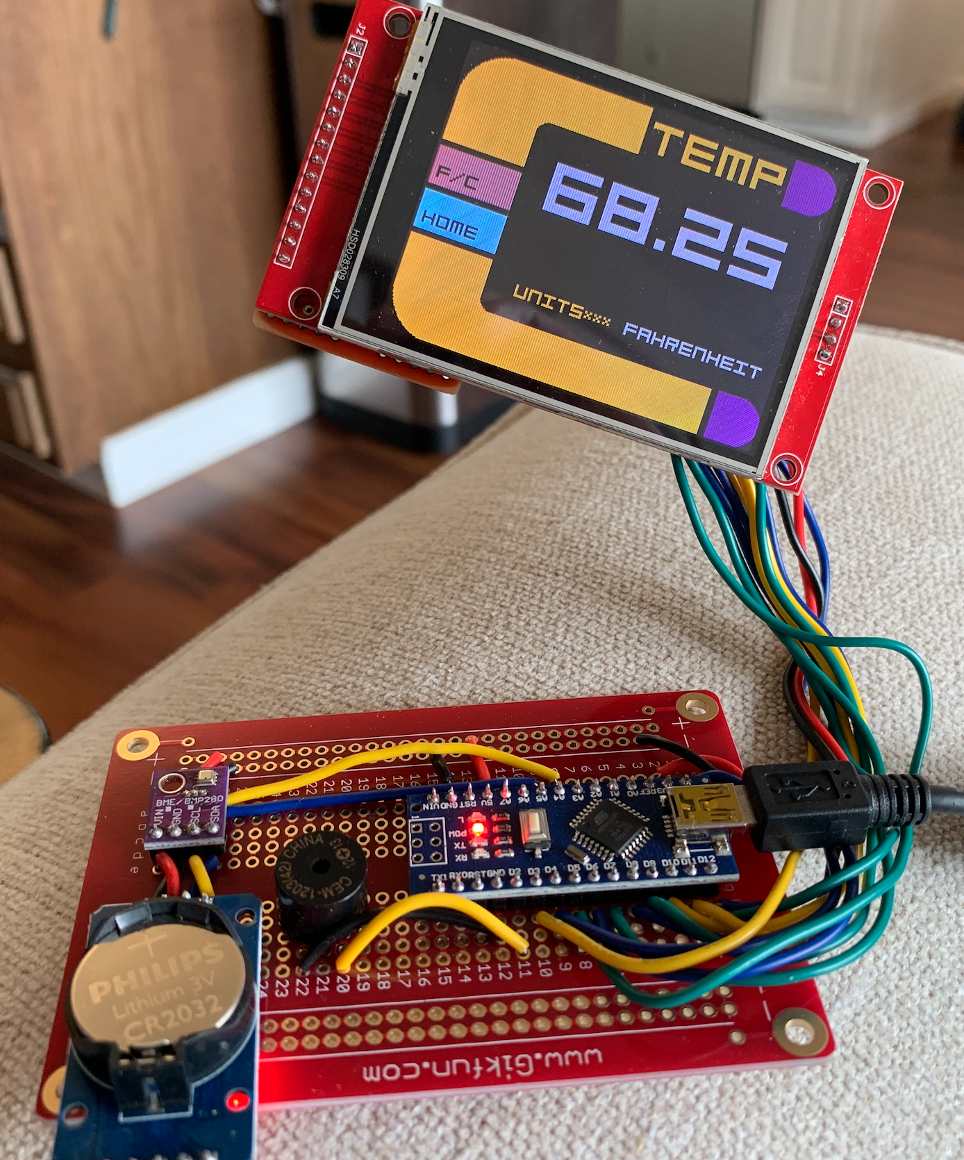
The Screen task runs every 10 ms and checks if a button was pressed on the touch screen. The task will update the screen according to the state transition diagram. The Time task runs every 60 seconds and updates the clock value on the Home Screen. The task is only active when the Home Screen is active. The Temperature task runs every 5 seconds and updates the temperature reading on the Temperature Screen. Like the Time task, it is only active when the Temperature Screen is active. I included some additional sub-tasks that convert the temperature reading between Fahrenheit and Celsius if the user presses the units button. Finally, the Alarm task runs every 60 seconds and checks if the RTC clock value is equal to the alarm time set by the user. The task is only active if the user has enabled an alarm on the Alarm Screen. When an alarm goes off, the piezo buzzer plays a tone and the user is prompted to either snooze or stop the alarm.
The biggest problem with this device is its speed. As I discussed earlier, the Adafruit Graphics Library does not allow for particularly fast screen rates, especially using an 8 MHz microcontroller. Based on the time taken to read the touch screen, I often need to press the screen for multiple seconds to give it enough time to register a button press. It would be much better to use an RTOS on a faster microcontroller to acheive more practicality. Nonetheless, the temperature sensor is accurate, so the device is reasonably successful in allowing me to monitor my immediate environment.
Now that I had a somewhat functional prototype, I wanted to see if I could compress all of the hardware into a smaller form factor. I switched from an Arduino Nano development board to a Wemos D1 Mini, which carries the much faster ESP8266 microcontroller. In addition, I downsized to a small OLED display with two buttons. While not as colorful, the display was driven via I2C, which required much less I/O pins from the microcontroller.
I was able to reduce the hardware to a single breadboard. The ESP8266 has built-in WiFi, which I could use to obtain the current time instead of with a Real Time Clock module.
I also designed an enclosure that closely mimicked the TV show prop design. The biggest problem with this design was the complexity of the internal geometry. With several angled and curved faces, it was difficult to acheive a logical positioning of the electronics that also fit into the tight enclosure. I also had to reconsider battery power, and struggled to figure out where to place a battery inside the device. Another major problem with this design is the hinge. The bottom clasp of the design has a lot of unused space, which would be perfect for a battery. However, 3D printing hinges that also allowed for wires to pass through would be incredibly complex.
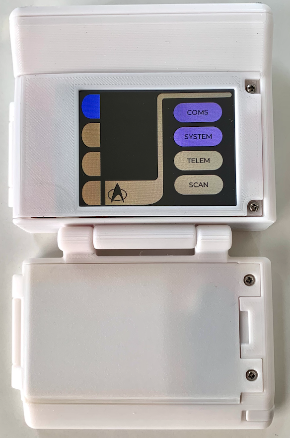
After struggling with the electronics in my first two prototypes, I learned the fundamentals of circuit board design in my coursework and senior project. I started by designing a "motherboard" that housed an ESP32 development board, a 2.8" touch screen, and a power management circuit. I included several expansion pins for the development board to allow for future integration with sensors. The plan is essentially to have a "core" device that can interface with other sensors in a modular fashion via I2C communication. The schematic is shown below.
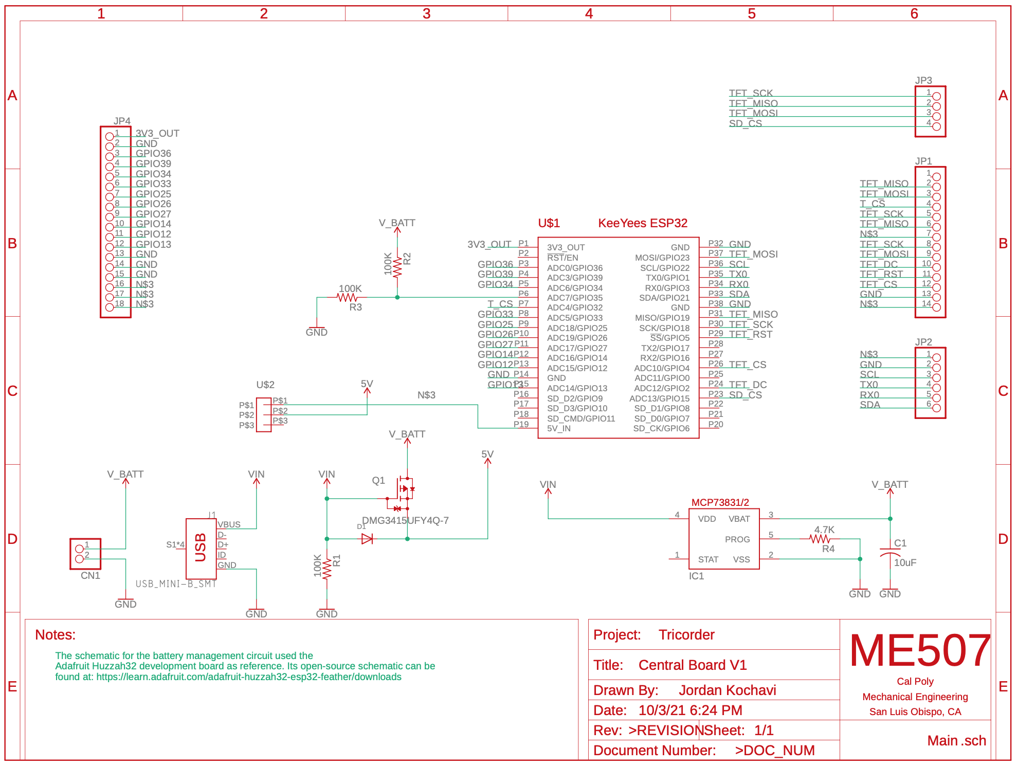
For the battery management, I wanted to be able to have the device seamlessly switch between battery and USB power as needed. This was accomplished with a p-channel MOSFET that will provide +5V to the ESP32 development board from either the battery or the USB. In addition, I also included a lithium-polymer charging circuit so that the battery will also be charged whenever the USB port receives power. I also tied the battery voltage to an ADC pin to measure the battery level. The ICs used in this schematic were taken from an open-source Adafruit Feather development board. I had considered just purchasing a development board with battery management, but given the complex geometry in the Tricorder enclosure, I wanted to design a custom development board where I could control the layout of the electronics.
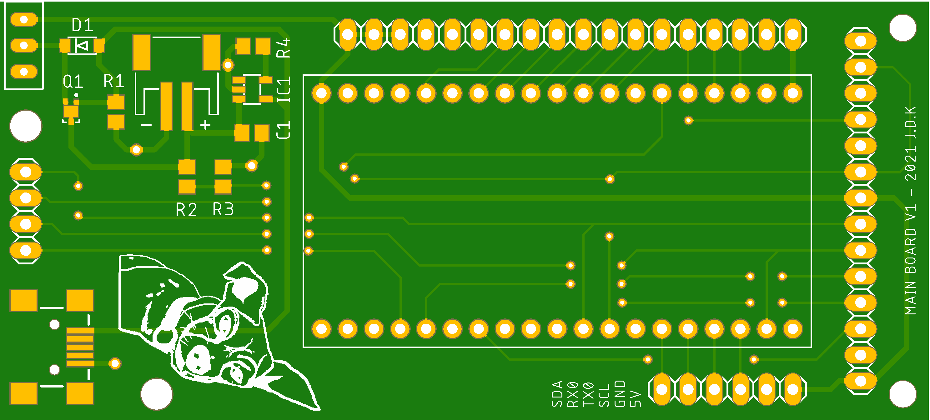
The printed circuit board design is shown above. The ESP32 development board, which is outlined in a large white rectangle, sits in the center of the PCB. The LCD screen fits directly over the PCB using the vertical header pins at the far right of the board. A mini USB port provides power to the board in the bottom left corner, and a two position switch turns the device on and off in the top left corner. A two-pin JST-PH connector allows for a battery to be easily connected, and its charging and power management circuit surrounds it. Finally, I included GPIO, serial, and I2C expansion pins that will allow me to connect the board to future sensors.
Unfortunately, the ongoing chip crisis severely restricted my choices of IC packages, so I was left with exceedingly small components that could only be assembled with SMD soldering. Also, many of the components were unavailable from online manufacturers like JLC PCB, so I had to source components separately from both Digikey and Mouser, and I had to do the SMD soldering myself.
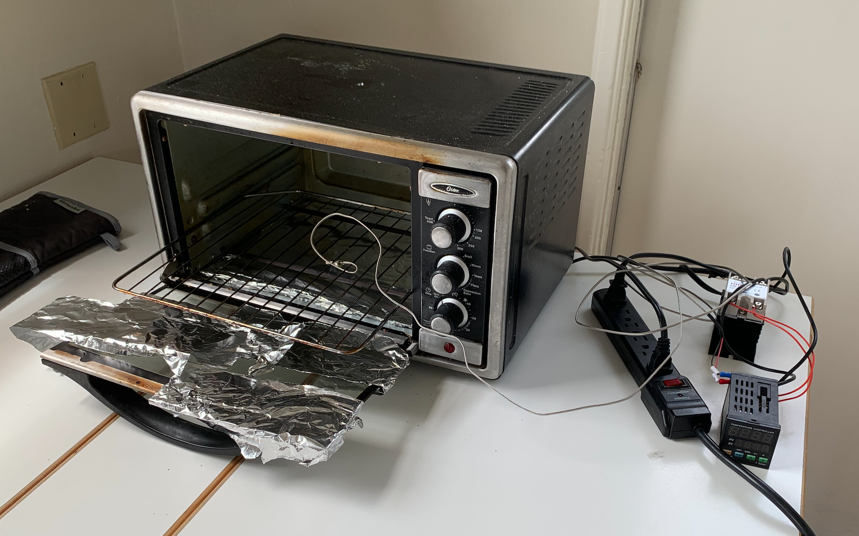
I sacrificed an old toaster oven that had a convection bake setting and connected it to a temperature controller. I placed a thermocouple inside the oven and heated the PCB until the solder paste reached its melting point.
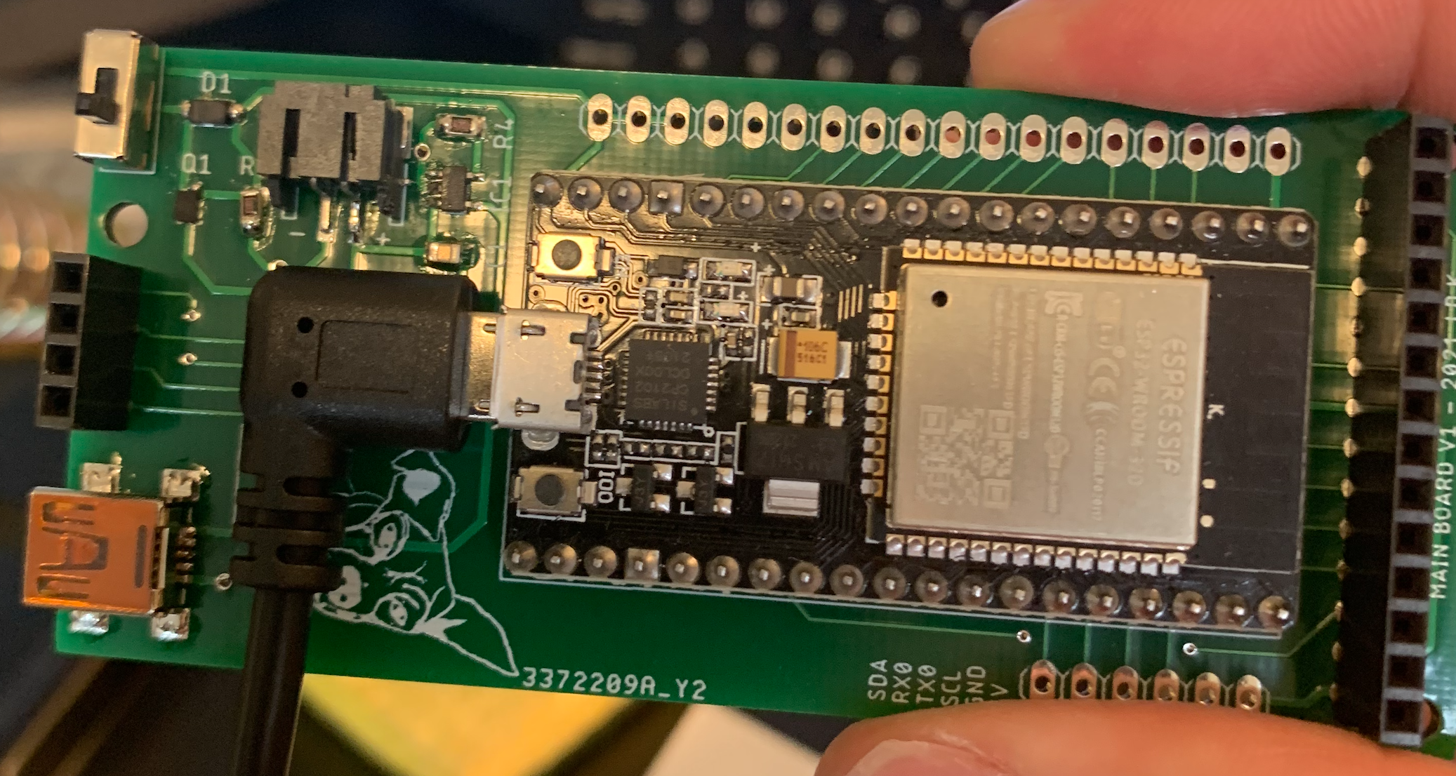
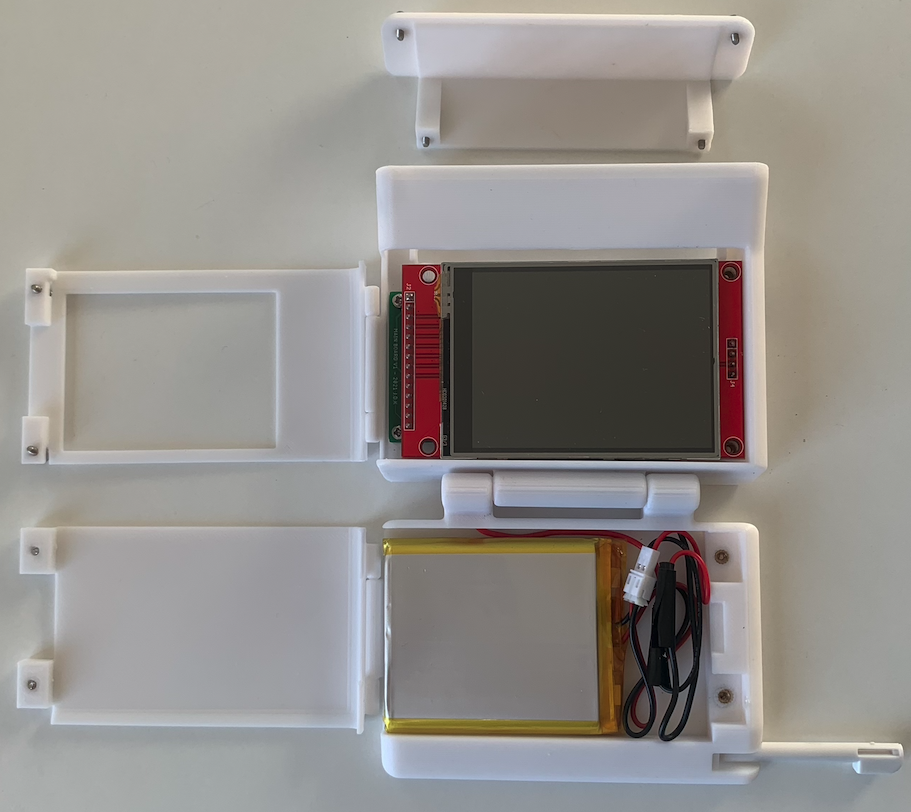
Next, I soldered the through-hole components with a soldering iron. Shown below, the completed PCB can be programmed with a micro USB cable that plugs into the ESP32 development board. Shown below, the screen fits directly above the PCB.
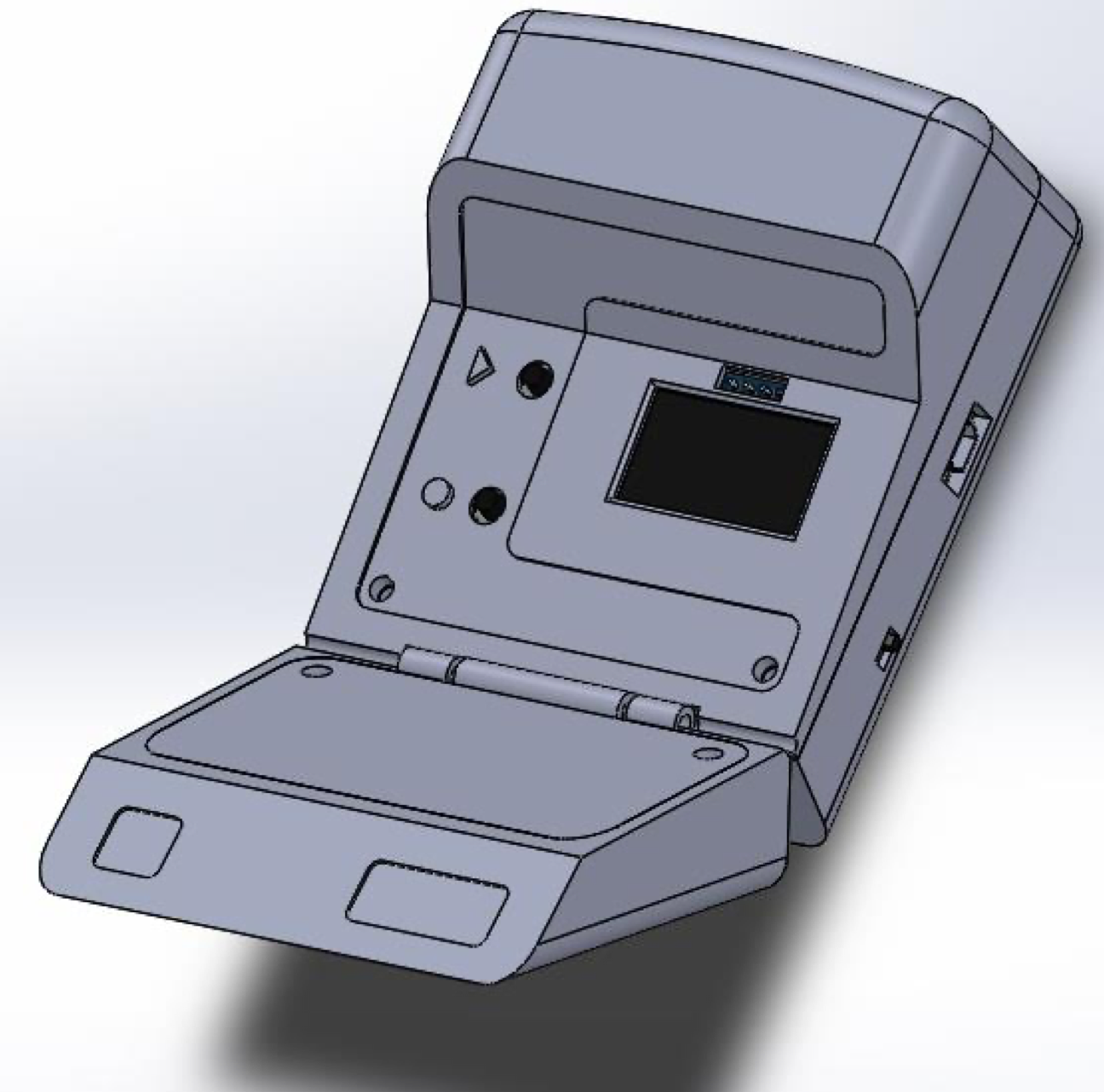
For the enclosure, I decided to abandon a strict adherance to the exact dimensions of the TV prop. It was more important that I design a hinged enclosure that had enough room for all of the electronics and allow wires to pass through the hinges.
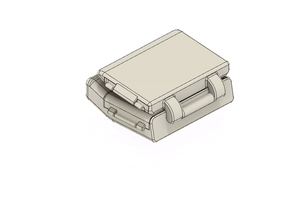
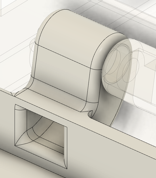
The enclosure was designed using Autodesk Fusion 360. It consists of a single "print-in-place" part with three hinges, as shown in the animation above. I added multiple hinges to this design in order to minimize assembly. Assembling several different pieces using fasteners can significantly lengthen the assembly process. If I had designed this enclosure to consist of three different pieces, I would need twice the amount of screws, which doubles the amount of time taken to compeltely disassemble the device. This way, I only need to unscrew two fasteners to gain access to the circuit board, and unscrew two more to access the battery. The design of the hinges required several iterations. The image below is a top-view of the hinge design.
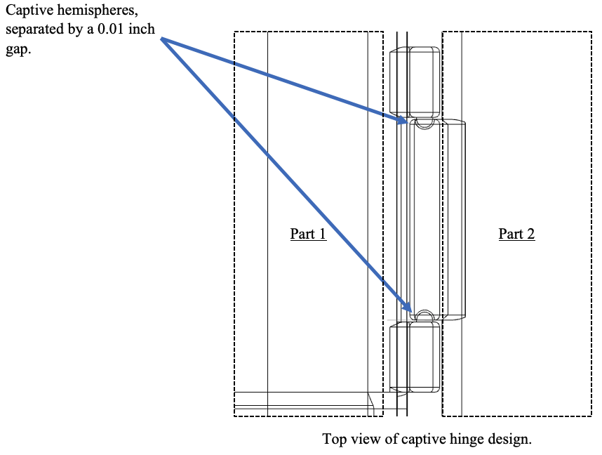
The dashed rectangles represent the two objects that are joined together by the hinge in the center. In the hinge design, Part 2 is sandwiched between Part 1 and held captive by two protruding hemispheres. Because of this "captive" state, Part 1 and Part 2 cannot be printed separately and assembled; instead, they must be printed as a single body. To accomplish this, I included a carefully calibrated gap between the hemispheres that join Part 1 and Part 2, which is indicated by the blue arrows above. A gap too large would result in an excessively loose hinge, while a gap too small would result in the two parts being fused together in the printing process. After several tests, I determined that a gap of 0.01 inches was the smallest gap that my Ender 3 Pro 3D printer could accomodate while allowing translation between the two hinged parts.
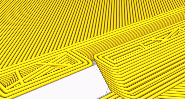
The animation above demonstrates how the hinge is printed. Layer-by-layer, the 3D printer extrudes the hemisphere out of Part 1 and into Part 2, thereby holding Part 2 captive.
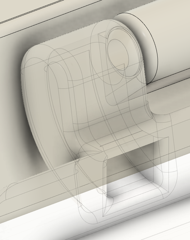
While this hinge design was effective for the two smaller hinges in the design, it would not work for the largest hinge, which is visible in the image above. Since the battery is located in the bottom half of the device, I had to find a way to route wires through the hinge to reach the electronics in the top half of the device. This adds an additional layer of complexity to the print-in-place hinge design.
In order to route wires through the print-in-place hinge, I started by increasing the size of the hinge to accomodate the thickness of two 22 AWG wires. I hollowed out the inside of the hinge to allow for a narrow cavity for the wires to pass through. The captive part, which is not visible in the image above, possesses similar protruding hemispheres to the other hinged designs, except with another small cavity, which is visible in the image below.
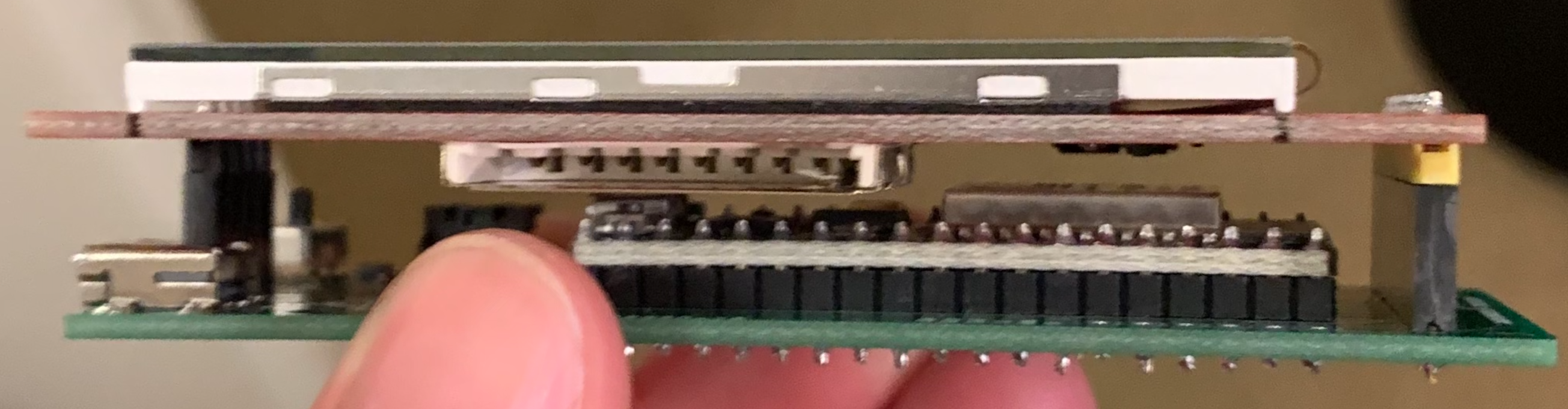
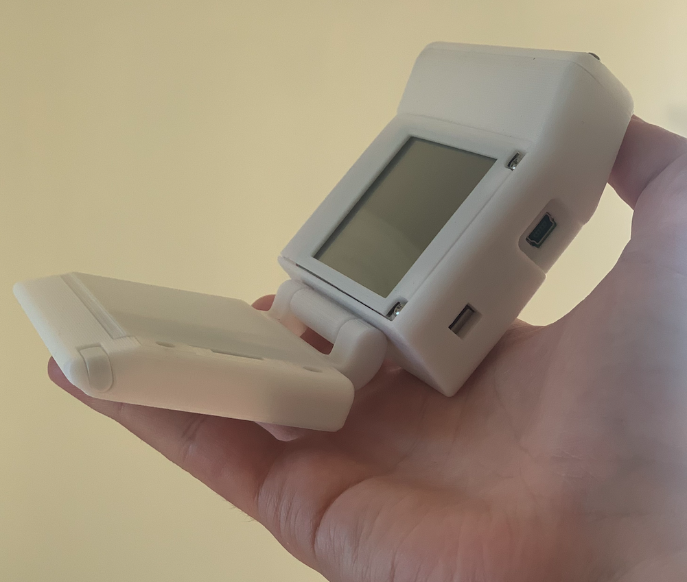
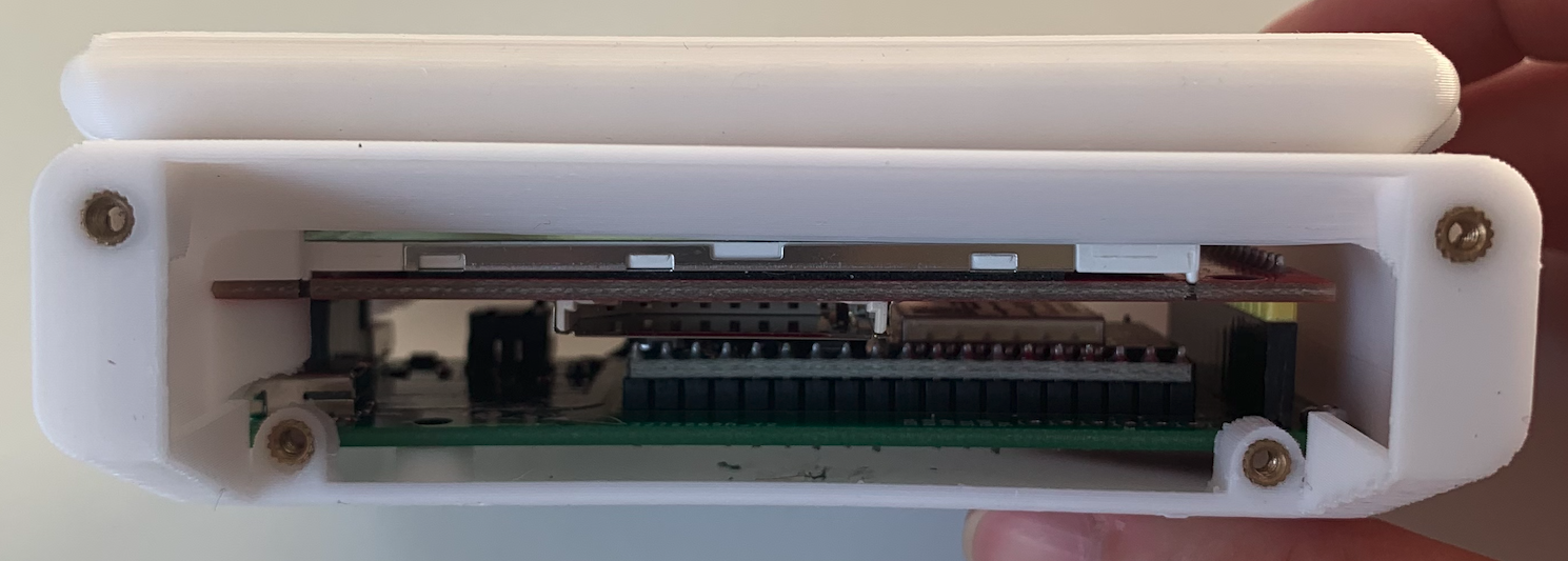
With the careful use of some tweezers, I was able to thread both battery wires through the hinge to reach the top half of the device. The image below highlights the various components inside the device.
The lower half of the device contains the battery, as well as the stylus that came with the touch screen module. The positive lead of the battery passes through the left half of the hinge, while the negative lead of the battery passes through the right half. While the majority of the device enclosure was printed as a single piece, I added one completely detached "hat" that is visible in the image above. The next step in this project is to design a second PCB that contains all the sensors that I want the device to interface with. Since this board has not yet been designed, I added an element of modularity to this enclosure, so I would only need to redesign a small portion of the device to accomodate future sensors.
Shown above, the sensor board will be mounted perpendicular to the LCD and main circuit board. This is the best location for sensor placement relative to the other electronics because the top of the device is the farthest location from the user's hands. An increased distance from the human user will reduce potential interference with sensor input. For example, if a temperature sensor were included on the sensor board, it would be directed away from the user and the other electronics, which would maximize its chance of measuring the true ambient environment temperature, rather than the user's body temperature or the temperature difference produced by the other electronics.